- 您现在的位置:买卖IC网 > Sheet目录2009 > MAX19713ETN+T (Maxim Integrated Products)IC ANLG FRNT END 56-TQFN
MAX19713
10-Bit, 45Msps, Full-Duplex
Analog Front-End
18
______________________________________________________________________________________
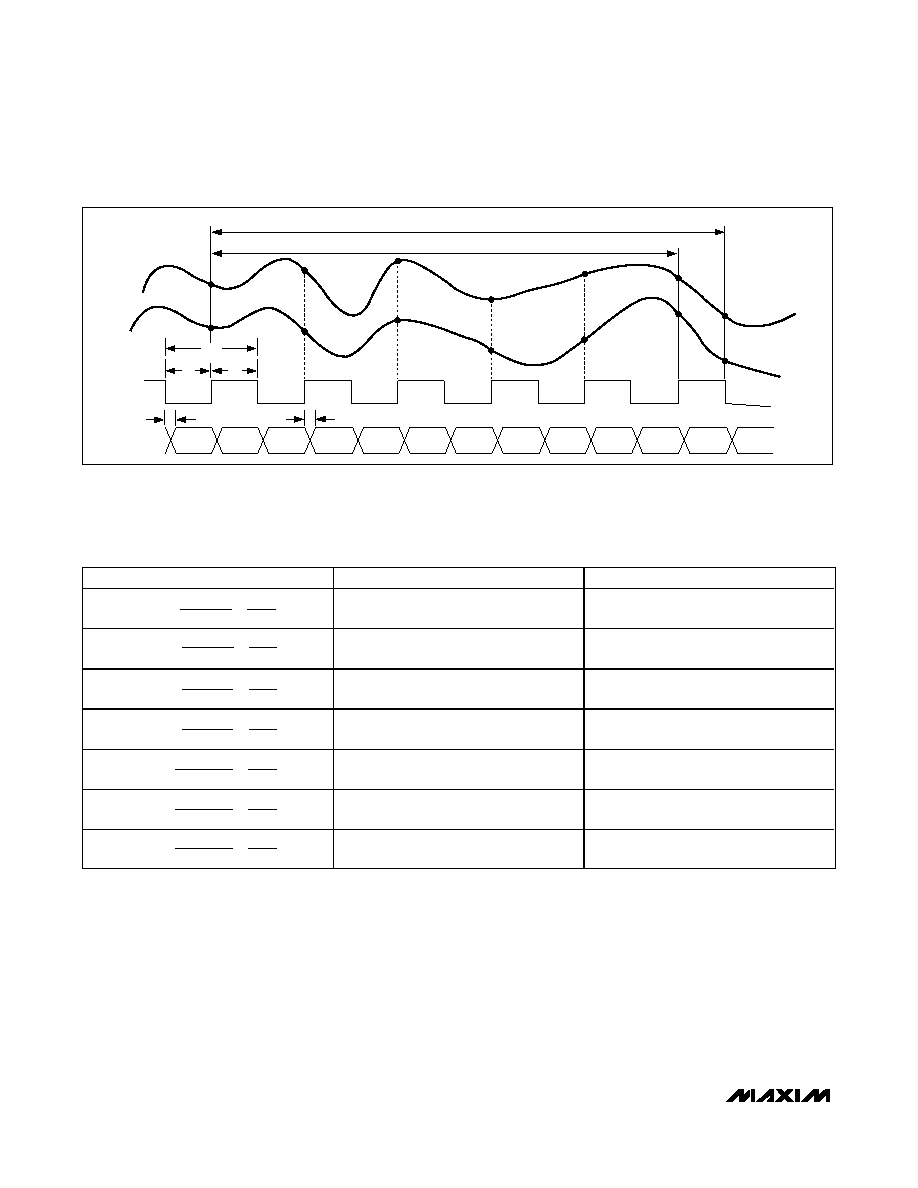
Figure 3. Rx ADC System Timing Diagram
tDOQ
tCL
tCH
tCLK
tDOI
5 CLOCK-CYCLE LATENCY (IA)
5.5 CLOCK-CYCLE LATENCY (QA)
D0–D9
D0Q
D1I
D1Q
D2I
D2Q
D3I
D3Q
D4I
D4Q
D5I
D5Q
D6I
D6Q
IA
QA
CLK
Table 2. Tx DAC Output Voltage vs. Input Codes
(Internal Reference Mode VREFDAC = 1.024V, External Reference Mode VREFDAC = VREFIN, VFS = 400 for 800mVP-P
Full Scale)
The Tx DAC outputs (IDN, IDP, QDN, QDP) are biased at
an adjustable common-mode DC level and designed to
drive a differential input stage with
≥ 70kΩ input imped-
ance. This simplifies the analog interface between RF
quadrature upconverters and the MAX19713. Many RF
upconverters require a 0.71V to 1.06V common-mode
bias. The MAX19713 common-mode DC bias eliminates
discrete level-setting resistors and code-generated level
shifting while preserving the full dynamic range of each
Tx DAC. The Tx DAC differential analog outputs can-
not be used in single-ended mode because of the
internally generated common-mode DC level. Table 2
shows the Tx DAC output voltage vs. input codes. Table
10 shows the selection of DC common-mode levels.
See Figure 4 for an illustration of the Tx DAC analog
output levels.
The Tx DAC also features an independent DC offset trim
on each ID–QD channel. This feature is configured
through the SPI interface. The DC offset correction is
used to optimize sideband and carrier suppression in the
Tx signal path (see Table 9).
DIFFERENTIAL OUTPUT VOLTAGE (V)
OFFSET BINARY (DA0–DA9)
INPUT DECIMAL CODE
11 1111 1111
1023
11 1111 1110
1022
10 0000 0001
513
10 0000 0000
512
01 1111 1111
511
00 0000 0001
1
00 0000 0000
0
V
FS
REFDAC
1024
1023
()
×
V
FS
REFDAC
1024
1021
1023
()
×
V
FS
REFDAC
1024
3
1023
()
×
V
FS
REFDAC
1024
1
1023
()
×
V
FS
REFDAC
1024
1
1023
()
×
V
FS
REFDAC
1024
1021
1023
()
×
V
FS
REFDAC
1024
1023
()
×
发布紧急采购,3分钟左右您将得到回复。
相关PDF资料
MAX271ENG+
IC FILTER LOWPASS PROG 24-DIP
MAX274ACWI+T
IC FILTER ANALOG 8TH-ORD 28SOIC
MAX281AEWE+
IC FILTER 5TH-ORD BESSEL 16-SOIC
MAX294CSA+
IC FILTER LOWPASS 8TH 8-SOIC
MAX295ESA+
IC FILTER LOWPASS 8-SOIC
MAX3634ETM+T
IC CLOCK PHASE ALIGNER 48-TQFN
MAX3676EHJ+T
IC CLOCK RECOVERY 32-TQFP
MAX3872ETJ+T
IC DATA RECOVERY W/AMP 32-TQFN
相关代理商/技术参数
MAX19713ETN+TGH7
功能描述:ADC / DAC多通道 10-Bit 45Msps Full-Duplex Analog Front-End RoHS:否 制造商:Texas Instruments 转换速率: 分辨率:8 bit 接口类型:SPI 电压参考: 电源电压-最大:3.6 V 电源电压-最小:2 V 最大工作温度:+ 85 C 安装风格:SMD/SMT 封装 / 箱体:VQFN-40
MAX19713ETN-T
功能描述:ADC / DAC多通道 RoHS:否 制造商:Texas Instruments 转换速率: 分辨率:8 bit 接口类型:SPI 电压参考: 电源电压-最大:3.6 V 电源电压-最小:2 V 最大工作温度:+ 85 C 安装风格:SMD/SMT 封装 / 箱体:VQFN-40
MAX19713EVCMODU
功能描述:ADC / DAC多通道 RoHS:否 制造商:Texas Instruments 转换速率: 分辨率:8 bit 接口类型:SPI 电压参考: 电源电压-最大:3.6 V 电源电压-最小:2 V 最大工作温度:+ 85 C 安装风格:SMD/SMT 封装 / 箱体:VQFN-40
MAX19713EVCMODU+
功能描述:数据转换 IC 开发工具 MAX19710/13 Eval Kit RoHS:否 制造商:Texas Instruments 产品:Demonstration Kits 类型:ADC 工具用于评估:ADS130E08 接口类型:SPI 工作电源电压:- 6 V to + 6 V
MAX19713EVKIT
功能描述:数据转换 IC 开发工具 RoHS:否 制造商:Texas Instruments 产品:Demonstration Kits 类型:ADC 工具用于评估:ADS130E08 接口类型:SPI 工作电源电压:- 6 V to + 6 V
MAX19713EVKIT+
功能描述:数据转换 IC 开发工具 MAX19710/13 Eval Kit RoHS:否 制造商:Texas Instruments 产品:Demonstration Kits 类型:ADC 工具用于评估:ADS130E08 接口类型:SPI 工作电源电压:- 6 V to + 6 V
MAX1971EEE
功能描述:直流/直流开关调节器 RoHS:否 制造商:International Rectifier 最大输入电压:21 V 开关频率:1.5 MHz 输出电压:0.5 V to 0.86 V 输出电流:4 A 输出端数量: 最大工作温度: 安装风格:SMD/SMT 封装 / 箱体:PQFN 4 x 5
MAX1971EEE+
功能描述:直流/直流开关调节器 Dual 180 Out 1.4MHz 750mA Step-Down RoHS:否 制造商:International Rectifier 最大输入电压:21 V 开关频率:1.5 MHz 输出电压:0.5 V to 0.86 V 输出电流:4 A 输出端数量: 最大工作温度: 安装风格:SMD/SMT 封装 / 箱体:PQFN 4 x 5